Extending CHIPOS with more CHIP-8 instructions
In which I learn 6800 assembly in order to hack CHIPOS.
This post is part of a series on writing an emulator for the DREAM 6800 computer. Read the DREAM 6800 posts and look at the emulator’s repository.
The source code and binary for the modified CHIPOS (“CHIPOSLO”) can be downloaded from the CHIPOSLO GitHub repository.
OK, this is a long post. There’s a table of contents to the right. I’ll get into the nitty-gritty of writing short 6800 assembly, and even though I’m an amateur on that subject, I’m apparently better at it than writing short posts.
Quick recap: The DREAM 6800 was created in 1978 by Michael J. Bauer, and it came with a small, 1024 byte operating system called CHIPOS. CHIPOS incorporates an interpreter for a bytecode VM called CHIP-8, which originally appeared on RCA’s CDP1802-based COSMAC VIP computer in 1977. You can read more about CHIP-8 on Wikipedia.
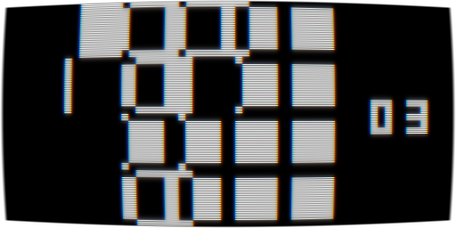
I’ve written a couple of CHIP-8 games myself, so I obviously wanted to see them run in my brand new emulator. However, I targeted those games for the original COSMAC VIP implementation, and that posed a problem for running them on the DREAM. This is my game Mini Lights Out in my DREAM emulator:
Undocumented CHIP-8 instructions
CHIP-8’s arithmetic and logic instructions are two bytes (like all instructions) and start with 8, followed by two nibbles that refer to two of the 16 “V” variables/registers, and ending with one nibble which denotes the operation. They look like this, where X and Y can be any hexadecimal number:
8XY0:VX = VY8XY1:VX = VX OR VY8XY2:VX = VX AND VY8XY4:VX = VX + VY(VF is set to 1 if there’s a carry, and 0 if there’s not)8XY5:VX = VX - VY(VF is set to 0 if there’s a borrow, and 1 if there’s not)
Notice the inverted use of the carry flag for the subtraction. That’s how the 1802’s carry flag worked, but it’s the opposite of the way it works on the 6800, necessitating some extra work later.
For the instructions that don’t specify what happens to VF, the resulting value in VF is undefined. 1802’s ALU would mangle it.
Due to the way the original CHIP-8 interpreter dispatches these instructions to the 1802’s ALU (details in this great blog post), it actually had four undocumented instructions. They are as follows:
8XY3:VX = VX XOR VY8XY6:VX = VY - VX(VF is set to 0 if there’s a borrow, and 1 if there’s not)8XY7:VX = VY >> 1(VF is set to the bit that’s shifted out)8XYE:VX = VY << 1(VF is set to the bit that’s shifted out)
Note that starting with the CHIP-48 and SUPER-CHIP interpreters in 1990,
8XY7and8XYEwere changed to doVX >>= 1andVX <<= 1respectively, ignoring the Y operand. For that reason, modern games should use the same V register as both operands to be cross-compatible.
The remaining instructions,
8XY8–8XYDand8XYF, do not elicit useful functionality.
These four undocumented instructions were discovered pretty early on, in 1978, and described in the COSMAC VIP’s newsletter VIPER (issue #2), but Bauer apparently wasn’t aware of them at the time he made the DREAM 6800. So his CHIP-8 interpreter in CHIPOS does not support them. My games, however, make heavy use of the shift instructions in particular.
This meant I couldn’t play my games in my DREAM emulator. I decided to take a little detour on my emulator development to see if I could cram them into CHIPOS. All I know about Motorola 6800 assembly is what I’ve learned from making this emulator, so this would be an interesting exercise.
The DREAM 6800’s CHIP-8 interpreter and monitor program, CHIPOS, fits in 1K of memory. Naturally, I wanted to squeeze in these extra instructions in that space. Was it doable?
CHIPOS code
You can download the CHIPOS code and ROM from Michael J. Bauer’s website.
Here’s a nice opcode table for 6800 assembly which I used as a reference during development.
The original CHIPOS interpreter uses the first nibble in the CHIP-8 instruction to index a jump table, and it jumps here when it encounters an opcode that starts with 8 (labels are Michael J. Bauer’s, comments are mine):
1
2
3
4
5
6
7
8
9
10
11
12
13
14
15
16
17
18
19
20
21
22
23
24
25
26
27
LETVV: LDAA VX    ; A will be used as result
       LDAB PIR+1 ; B = final byte of instruction
       ANDB #$0F  ; Pseudo-"opcode" in final nibble
       BNE  LETV1 ; 8XY0
       LDAA VY    ; VX = VY
LETV1: DECB
       BNE  LETV2 ; 8XY1
       ORAA VY    ; VX |= VY (OR)
LETV2: DECB
       BNE  LETV4 ; 8XY2
       ANDA VY    ; VX &= VY (AND)
LETV4: DECB
       DECB
       BNE  LETV5 ; 8XY4
       CLR  VF    ; VF = 0
       ADDA VY    ; VX += VY
       BCC  LETV5 ; Check carry
       INC  VF    ; VF = 1 (overflow)
LETV5: DECB
       BNE  PUTVX ; 8XY5
       CLR  VF    ; VF = 0
       SUBA VY    ; VX -= VY
       BCS  PUTVX ; VX < VY? (unsigned)
       INC  VF    ; VF = 1
PUTVX: LDX  VXLOC
       STAA 0,X   ; Replace VX with result
       RTS        ; Return
This is basically a switch/case statement with fall through. First it sets up a couple of things: It loads the argument VX into accumulator A, and the last nibble of the CHIP-8 instruction into accumulator B. Then, if B is equal to zero (instruction 8XY0), it sets A equal to VY. Otherwise, it decrements B, and if that makes it equal to zero, it will execute 8XY1 and load A with the result of OR-ing A with VY. This goes on all the way to the bottom, where it finally loads VX with A and returns. Notice how it decrements B twice after checking 8XY2, explicitly skipping the undocumented instruction 8XY3.
So, how could I squeeze in checks for 8XY3, 8XY6, 8XY7 and 8XYE here, and the code needed to execute those instructions, while not using a single byte? I tried a couple of approaches.
First try: Shaving off bytes
In the code block above, LDAB PIR+1 sets the B accumulator to the second byte of the CHIP-8 instruction (which in this case is used as a counter to execute the correct instruction based on the last nibble). I noticed quickly that many of the destinations from the major jump table did this, since a lot of instructions have operands in that last nibble. None of them expected B to hold any particular value first. So I moved the LDAB PIR+1 to occur before the jump table, and removed it from all the destinations.
This actually turned out to save me a lot of bytes. It also let me simplify that initial jump table a little; some of the jumps were to small routines, like the one for VX = KK (where KK is a one-byte constant) only loaded A with that last nibble, and then immediately branched to the PUTVX routine, for example. Now that could be a simple jump to PUTVX.
I changed some other things too. To give one (perhaps idiomatic?) example, I changed this:
1
2
3
4
5
6
7
8
9
10
11
12
13
14
15
EXCALL: LDAB 	PIR         ; GET INSTR FIRST BYTE
        BNE     CALL        ; IF != 0, CALL IT
        LDAA    PIR+1       ; GET INSTR LAST BYTE
        CMPA  	#$E0        ; IF 00E0 (CLEAR SCREEN)
        BEQ     ERASE
        CMPA  	#$EE        ; IF 00EE (RETURN)
        BEQ     RETDO
        RTS                 ; NOP, BACK TO FETCH
ERASE:  CLRA                ; WRITE ZEROS TO SCREEN
        LDX 	#DISBUF     ; POTNT TO DISPLAY BUFF
FILL:   STAA 	0,X         ; FILL SCREEN WITH ACC-A
        INX
        CPX  	#ENDBUF     ; DONE?
        BNE     FILL
        RTS
To this:
1
2
3
4
5
6
7
8
9
10
11
12
13
EXCALL: LDAB 	PIR         ; GET INSTR FIRST BYTE
        BNE     CALL        ; IF != 0, CALL IT
        CMPA  	#$EE        ; IF 00EE (RETURN)
        BEQ     RETDO
        CMPA  	#$E0        ; IF 00E0 (CLEAR SCREEN)
	BNE     RET         ; NOP, BACK TO FETCH
ERASE:  CLRA                ; WRITE ZEROS TO SCREEN
        LDX     #DISBUF     ; POTNT TO DISPLAY BUFF
FILL:   STAA    0,X         ; FILL SCREEN WITH ACC-A
        INX
        CPX     #ENDBUF     ; DONE?
        BNE     FILL
RET:    RTS
Notice how I replace two branches and a return with two branches, where one of them is just a branch to an existing return. Seems silly, but you can’t conditionally return on the MC6800, so this saves one whole byte (plus the aforementioned LDAA PIR+1).
When all was said and done, it actually looked like I had room to insert all the new cases in the original switch. It ended up looking like this:
1
2
3
4
5
6
7
8
9
10
11
12
13
14
15
16
17
18
19
20
21
22
23
24
25
26
27
28
29
30
31
32
33
34
35
36
37
38
39
LETVV: TAB        ; B = final byte of instruction
       LDAA VY    ; A will be used as result (preloaded with VY now)
       ANDB #$0F  ; Pseudo-"opcode" in final nibble
       BEQ  PUTVX ; 8XY0
       CLR  VF    ; VF = 0
LETV1: DECB
       BNE  LETV2 ; 8XY1
       ORAA VX    ; VY |= VX (OR)
LETV2: DECB
       BNE  LETV3 ; 8XY2
       ANDA VX    ; VY &= VX (AND)
LETV3: DECB
       BNE  LETV4 ; 8XY3
       EORA VX    ; VY ^= VX
LETV4: DECB
       BNE  LETV5 ; 8XY4
       ADDA VX    ; VY += VX
       BCS  INCVF ; VF = 1 (overflow)
LETV5: DECB
       BNE  LETV6 ; 8XY5
       LDAA VX
       SUBA VY    ; VX -= VY
       BCC  INCVF ; VF = 1 (no borrow)
LETV6: DECB
       BNE LETV7  ; 8XY6
       LSRA       ; VY >>= 1
       BCS INCVF  ; VF = 1 (overflow)
LETV7: DECB
       BNE LETVE  ; 8XY7
       SUBA VX    ; VY -= VX
       BCC INCVF  ; VF = 1 (no borrow)
LETVE: SUBB #7    ; skip 8XY8 through 8XYD
       BNE PUTVX  ; 8XYE
       ASLA       ; VY <<= 1
       BCC PUTVX  ; VF = 1 (overflow)
INCVF: INC VF
PUTVX: LDX VXLOC
       STAA 0,X   ; Replace VX with result
       RTS        ; Return
The beginning is slightly different. The A accumulator now starts off with the last nibble of the instruction, but I need A for the result that will eventually be put in VX, so I transfer it to B with a TAB. I could have changed PUTVX to use B instead of A, but a lot of routines call PUTVX, including some routines that put their results in A.
Speaking of the result that will eventually end up in VX: Many of the instructions are symmetrical concerning the operands (VX &= VY is equivalent to VX = VY & VX, for example), and as for the ones which are not, with the new shift instructions there are actually more instructions that operate on VY (VX = VY - VX, VX = VY << 1 and VX = VY >> 1) than VX (only VX -= VY), so I now do LDAA VY up top instead.
I also shortened the VX = VY instruction, and do CLR VF on the top as well – VF was changed by all the arithmetic/logic instructions in the original COSMAC VIP interpreter, even when the result was undefined, so I do it here too (hoping no CHIP-8 games for DREAM rely on the opposite, and probably being wrong). Likewise, setting VF to 1 is moved to the bottom.
So there you have it: I’d successfully shaved off as many bytes as I could in CHIPOS, and inserted the missing instructions in the handler. Then the only thing that remains is to assemble it and – oh.
1025 bytes. One byte over budget.
Take two: Dynamic programming
Try as I might, I wasn’t able to find another byte to optimize away. And not all bytes are equal; if possible, I wanted to stay compatible with CHIPOS’s subroutines and calling sequences (CHIPOS provides several of its subroutines for use by DREAM programs and games). There probably is one somewhere, but I can’t find it. If you do, please leave a comment, because the above code is much cleaner and elegant than the monstrosity I’m about to unveil.
I noticed that many of the CHIP-8 instructions here map cleanly to a single MC6800 instruction each. However, some need an operand (VY before, VX in my revised routine), so that’s two bytes, and some don’t need an operand. Hardcoded jump tables can get pretty big, since each case needs a return. I tried to make a jump table, but that approach was much larger than the 1025 byte switch/case above. (It was 1040 bytes when I abandoned it.)
Instead of a jump table, I thought: What if I had a table of the 6800 instructions that CHIP-8 maps to… And then instead of putting the operand and everything else that’s needed in there, since it will be almost the same for each case, I build a jump target in RAM? I have no idea if this wass common to do back in the day, but it ended up pretty nicely. Here’s the table:
1
2
3
4
5
6
7
8
9
JUMP8:  .byte $96 ;LDAA 8XY0
        .byte $9A ;ORAA 8XY1
        .byte $94 ;ANDA 8XY2
        .byte $98 ;EORA 8XY3
        .byte $9B ;ADDA 8XY4
        .byte $90 ;SUBA 8XY5
        .byte $48 ;ASLA 8XY6
        .byte $90 ;SUBA 8XY7
        .byte $44 ;LSRA 8XYE
This is just a lookup table, where entry 0 holds the byte code for LDAA (direct addressing) which is used by 8XY0, entry 1 is 8XY1 with ORAA, etc. Then I could just use accumulator B (the final nibble of the CHIP-8 instruction) to look up the correct opcode in the table and stick it somewhere.
Of course, it’s not quite that easy. As above, entries 0 through 5 take VX as an operand, 7 takes VY, and 6 and E don’t take an operand at all. I needed to put the opcode into RAM, followed by one or no operand, followed by an RTS to get back.
So I thought, what if I move VY to the memory location (in zero page, so an 8-bit address) that is equal to the byte code for RTS, and put two RTS in a row? RTS is $39. Unfortunately, CHIPOS uses that location to store all the V variables, and I didn’t want to move them in case some other programs might rely on them. I couldn’t move VY to the memory location that has the same binary value as a NOP either, since that’s $01 which is used by the interrupt vector. I don’t use the overflow flag for anything, though, and the instruction CLV (clear overflow flag) is opcode $0A. That address is used by CHIPOS as temporary storage for digit patterns, so I could move that easily. I put it at $0080, which is available scratch space.
Now I could put the opcode from the table above at address $0040 (semi-randomly selected), followed by an $0A that will either be VY’s memory location or a “NOP”-like CLV instruction, followed by a $39 for RTS. Boom!
Not so fast. What do I do about the hole in the table between entry 6 and entry E? I could just fill them with 8 bytes of garbage (or maybe a useful subroutine), but I needed to fill them with something, otherwise the lookup wouldn’t work. Unless… What’s that right below PUTVX?
1
2
3
RANDOM: LDAA #$C0
        STAA RNDX
        INC  RNDX+1
A routine for generating a new random number. Let’s count bytes; RNDX+1 appears right at the location of entry $E if I remove it from the table. LSRA has opcode $44, so I moved RNDX from location $002C to $0043. Tada! Of course, this means that the CHIP-8 instructions 8XY8 through 8XYD plus 8XYF (invalid instructions) would all make interpreter crash and burn utterly, but I figured that was OK.
Now we need to set VF, CHIP-8’s flag register, based on the 6800 carry flag. In the switch/case approach, I just cleared VF at the start, and set it in the cases that needed it. That cost a lot of bytes! Now that we do a single jump, we can actually do this instead, and not mangle VF when we don’t need to:
1
2
3
        ROR  VF    ; save VF in carry
        JSR  $0040 ; dispatch to RAM routine
        ROL  VF    ; load carry into VF
After executing the RAM routine, the carry flag will either be the one I saved before, or it’ll be the new one in those cases that CHIP-8 cares about it, since there’s a one-to-one correspondence between 6800 instructions that touch carry and CHIP-8 instructions that touch VF.
Well, almost. MC6800’s SUB instruction sets carry on overflow, while CHIP-8 clears it. We’re not out of the woods yet! This turned out to be the most costly thing to take care of, because I didn’t find a better way than to simply check for each case. Luckily I could kill two birds with one stone, and use this check to also do another thing: Switch the operand for 8XY7, which does a VX = VY - VX.
The final blob ended up looking like this:
1
2
3
4
5
6
7
8
9
10
11
12
13
14
15
16
17
18
19
20
21
22
23
24
25
26
27
28
29
30
31
32
33
34
35
36
37
38
LETVV: TAB         ; B = final byte of instruction
       LDAA VY     ; A = result (preloaded with VY)
       ANDB #$0F   ; Pseudo-"opcode" in final nibble
       BEQ  PUTVX  ; 8XY0
       LDX  #$0A39 ; Load X with the sequence VX RTS
LETV5: CMPB #$05   ; 8XY5
       BNE  LETV7
       LDAA VX     ; Swap operand to VX
       LDX  #$2F7E ; Load X with the sequence VY JMP
LETV7: CMPB #$07   ; 8XY7
       BNE  done
       LDX  #$0A7E ; Load X with the sequence VX JMP
LETV:  STX  $0041  ; Store X at address $0041
       LDX  #INVC  ; Load X with address to invert carry
       STX  $0043  ; Store X at address $0043
FINDV: INX         ; Loop to find byte in lookup table
       DECB
       BNE  loop
       LDAB 3,X    ; B = address in X, plus an offset of 3
       STAB $0040  ; Store X's operation byte at $0040
       ROR  VF     ; Store VF in carry flag
       JSR  $0040  ; Dispatch to the RAM routine we built
       ROL  VF     ; Load VF from carry flag
PUTVX: LDX  VXLOC
       STAA 0,X    ; Replace VX with result
       RTS         ; Return from this whole thing
INVC:  ROLB        ; Invert carry if needed
       INCB
       RORB
       RTS
JUMP8: .byte $9A   ; ORAA 8XY1
       .byte $94   ; ANDA 8XY2
       .byte $98   ; EORA 8XY3
       .byte $9B   ; ADDA 8XY4
       .byte $90   ; SUBA 8XY5
       .byte $44   ; LSRA 8XY6
       .byte $90   ; SUBA 8XY7
      ;.byte $48   ; ASLA 8XYE (byte found in code below)
Whoo boy. Okay. So we build a subroutine in zero-page RAM that consists of the opcode for the instruction we want at $0040, followed by $0A which is the address of VX for those instructions that require that or it’s CLV for those that don’t or it’s $2F for VY since one instruction requires that, followed by either a $39 to return or a $7E to jump to INVF. Then we call that thing.
Doesn’t look like much, but that’s not important. The moment of truth: Time to assemble this baby…
Success
1024 bytes! I’d done it!
Building instructions in RAM like a crazy person only saved me one byte compared to the switch/case, but it was one crucial byte.
Let’s fire up my Mini Lights Out game and see if all the work paid off. CHIPOS runs, and lo and behold:
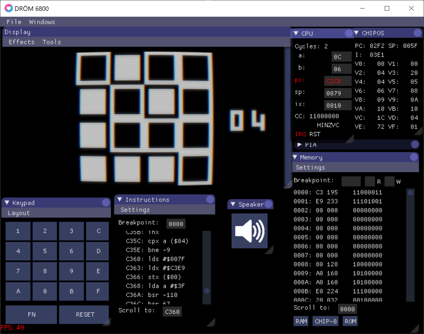
Beautiful. As a bonus for reading all of this you get to see the clunky UI of my emulator so far too. Time to get back to working on that!
I decided to call my version of CHIPOS “CHIPOSLO”, named after my home town Oslo, Norway and also short for “CHIPOS with Logical Operators”. Michael J. Bauer graciously released CHIPOS into the public domain, so here’s CHIPOSLO’s GitHub repository.
You can view the full diff between Michael’s CHIPOS and my modifications there (I didn’t cover all the details in this blog post).